File:Reverse-Biased pn Junction.svg

Size of this PNG preview of this SVG file: 400 × 225 pixels. Other resolutions: 320 × 180 pixels | 640 × 360 pixels | 1,024 × 576 pixels | 1,280 × 720 pixels | 2,560 × 1,440 pixels.
Original file (SVG file, nominally 400 × 225 pixels, file size: 14 KB)
|
|
This is a file from the Wikimedia Commons |
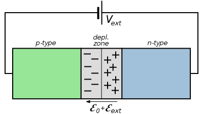
| Description | Diagram of a pn junction under forward bias the resultant electric field, , the depletion zone, the space charges, and the types of semiconductor. | ||
| Date | |||
| Source | Own drawing, done in Inkscape. | ||
| Author | inductiveload | ||
| Permission (Reusing this file) |
|
||
| Other versions |
 |


|
This SVG file contains embedded text that can be translated into your language, using any capable SVG editor, text editor or the SVG Translate tool. For more information see: About translating SVG files. |
File history
Click on a date/time to view the file as it appeared at that time.
| Date/Time | Thumbnail | Dimensions | User | Comment | |
|---|---|---|---|---|---|
| current | 01:53, 20 February 2007 | | 400 × 225 (14 KB) | Inductiveload | {{Information |Description=Diagram of a pn junction under forward bias the resultant electric field, <math>\mathcal{E}_0+\mathcal{E}_{ext}</math>, the depletion zone, the space charges, and the types of semiconductor. |Source=Own drawing, done in Inkscape |
File usage
The following page uses this file:
Global file usage
The following other wikis use this file:
- Usage on fr.wikibooks.org