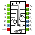
File:4073 Pinout.svg

Size of this PNG preview of this SVG file: 220 × 220 pixels. Other resolutions: 240 × 240 pixels | 480 × 480 pixels | 768 × 768 pixels | 1,024 × 1,024 pixels | 2,048 × 2,048 pixels.
Original file (SVG file, nominally 220 × 220 pixels, file size: 74 KB)
File history
Click on a date/time to view the file as it appeared at that time.
| Date/Time | Thumbnail | Dimensions | User | Comment | |
|---|---|---|---|---|---|
| current | 20:34, 21 March 2023 |  | 220 × 220 (74 KB) | Sheldrake | Corrected label of Pins 13 and 12 to A3 and B3 |
| 20:04, 21 March 2023 |  | 220 × 220 (74 KB) | Sheldrake | Corrected label of Pin 6 to Q1 | |
| 23:17, 21 September 2009 |  | 220 × 220 (74 KB) | Inductiveload | {{Information |Description={{en|1=Pinout diagram of the 4073 triple 3-input AND gate logic IC.}} |Source=Own work by uploader |Author=Inductiveload |Date=2009-09-22 |Permission={{PD-self}} |other_versions= }} [[Category:IC Pinout D |
File usage
The following page uses this file: